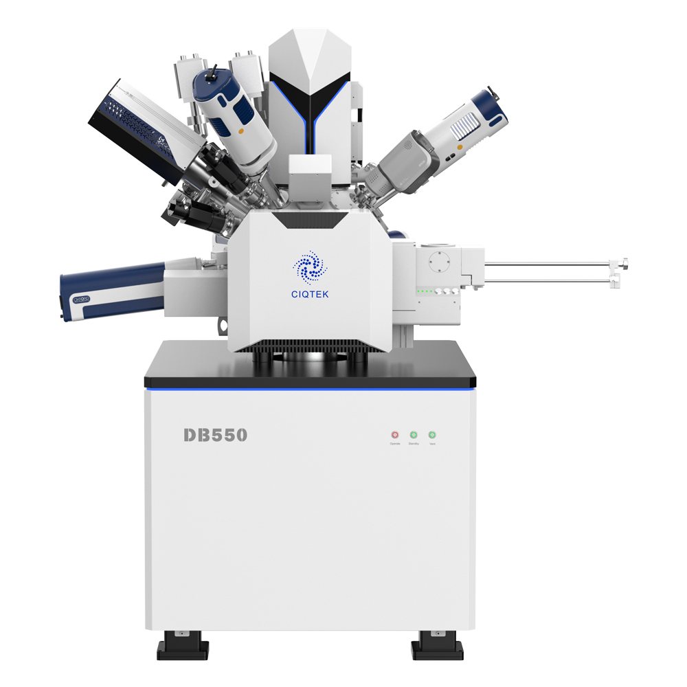
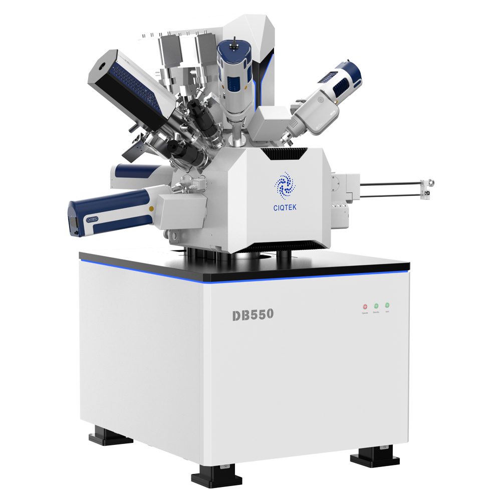
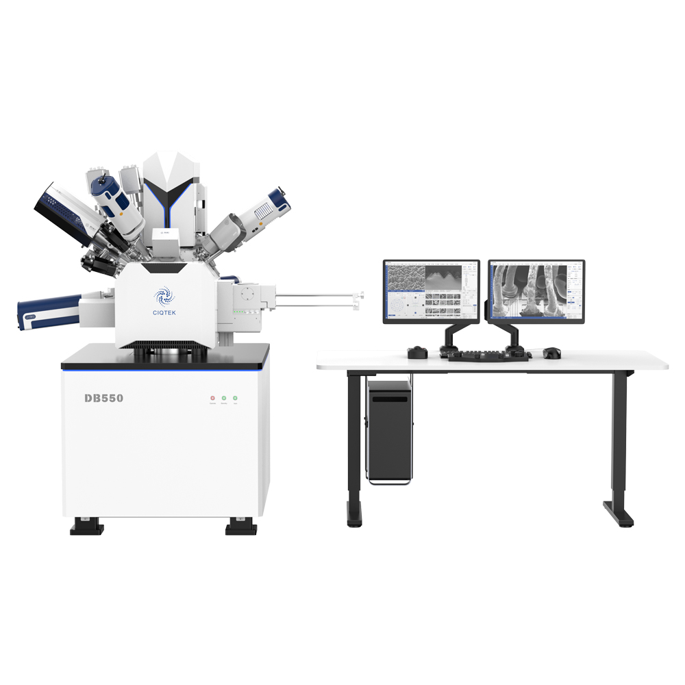
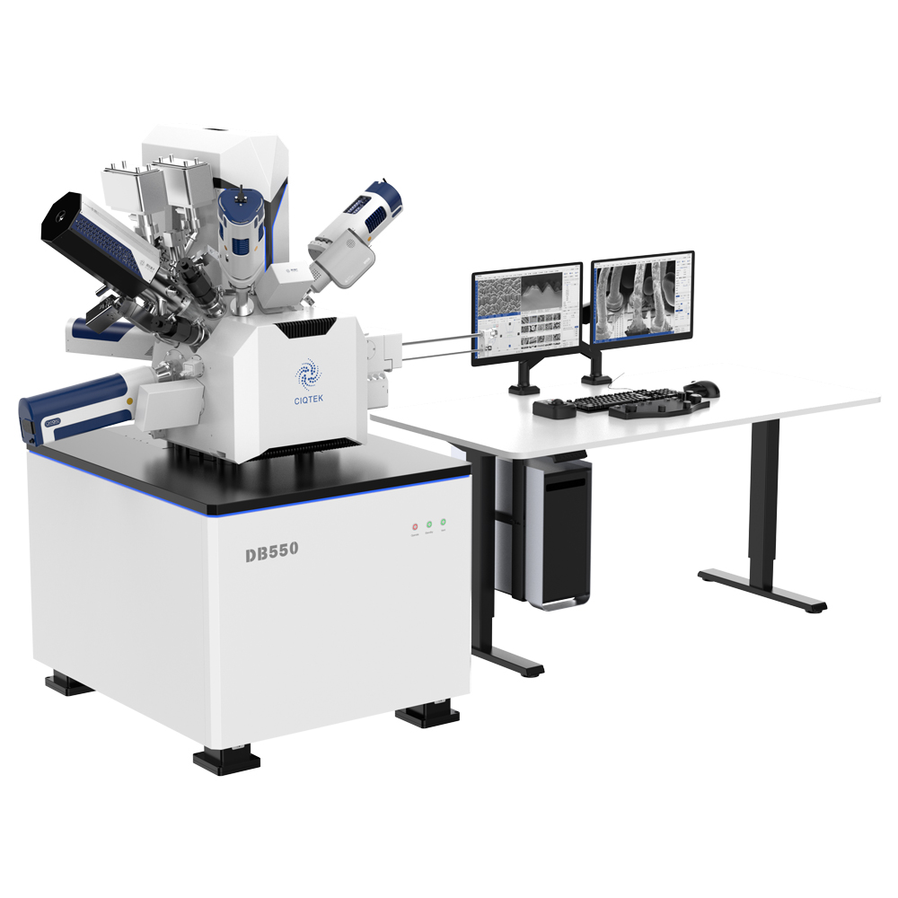
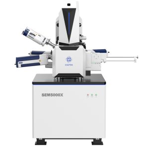
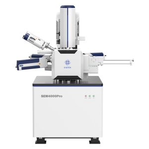
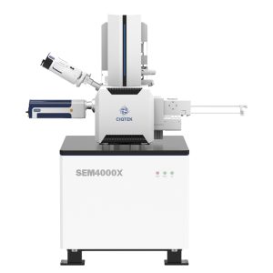
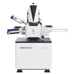
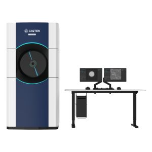
CIQTEK FIB-SEM DB550
Field Emission Scanning Electron Microscope (FE-SEM) with Focused Ion Beam (FIB) Columns.
The CIQTEK DB550 Focused Ion Beam Scanning Electron Microscope (FIB-SEM) has a focused ion beam column for nano-analysis and specimen preparation. It utilises “super tunnel” electron optics technology, low aberration and non-magnetic objective design, and has the “low voltage, high resolution” feature to ensure its nanoscale analytical capabilities.
The ion columns facilitate a Ga+ liquid metal ion source with highly stable and high-quality ion beams to ensure nanofabrication capabilities. The CIQTEK DB550 is an all-in-one nano-analysis and fabrication workstation with an integrated nano-manipulator, gas injection system, and user-friendly GUI software.
- “SuperTunnel” Electron Optics Technology
- Gallium Ion Beam
- Excellent Expandability
- Integrated Gas Injection System
- Integrated Nano-manipulator
- Specimen Exchange Loadlock (8 inches compatible)
Key Features:
“Super Tunnel” electron optics column technology/in-column beam deceleration. Decrease spatial charging effect, ensuring low voltage resolution performance.
Crossover-free in the electron beam path. Effectively reduce lens aberrations and improve resolution.
Electromagnetic & electrostatic compound objective lens. Reduce aberrations, significantly improve resolution at low voltages, and enable observation of magnetic samples.
Water-cooled constant-temperature objective lens. Ensure the stability, reliability, and repeatability of the objective lens performance.
Variable multi-hole aperture switching system by electromagnetic beam deflection. Automatic switching between apertures without mechanical motion allows fast switching among various imaging modes.
Techniques:
Focused Ion Beam (FIB) Column
- Resolution: 3 nm@30 kV
- Probe current: 1 pA to 65 nA
- Acceleration voltage range: 0.5 kV to 30 kV
- Ion source exchange interval: ≥1000 hours
- Stability: 72 hours of uninterrupted operation
Nano-manipulator
- Chamber internally mounted
- Three-axis all-piezoelectrically driven
- Stepper motor accuracy ≤10 nm
- Maximum travel speed 2 mm/s
- Integrated control system
Ion Beam-Electron Beam Collaboration
Gas Injection System
- Single GIS design
- Various gas precursor sources are available
- Needle insertion distance ≥35 mm
- Motion repeatability ≤10 μm
- Heating temperature control repeatability ≤0.1°C
- Heating range: room temperature to 90°C (194°F)
- Integrated control system
Applications:
Semiconductors – In the semiconductor industry, IC chips may encounter various failures. Various methods are used to analyse the chips to improve reliability. In particular, focused ion beam (FIB) analysis is reliable. Specimen Characterisation / Micro-Nano Fabrication / Cross-section Analysis / TEM Specimen Preparation / Failure Analysis.
New Energy Industries – Observing and analysing material cross-sections for research and process development. Morphology Observation / Particle Size Analysis / Cross-section Analysis / Composition and Phase Analysis / Failure Analysis of Lithium-ion Battery Material / TEM Sample Preparation.
Ceramic Materials – Material analysis: The FIB-SEM system can perform high-precision micro-nano machining and imaging of ceramic materials, combined with various signal detection modes such as backscattered electrons (BSE), energy-dispersive X-ray spectroscopy (EDX), Electron Backscattered Diffraction Pattern (EBSD), and secondary ion mass spectrometry (SIMS), to study the material in micro to nano-scale with three-dimensional space in depth.
Alloy Materials – To increase the strength, hardness, toughness, etc., of metals, other substances such as ceramics, metals, fibres, etc., are added into the metal using methods such as metallurgy, casting, extrusion, etc., which are called reinforced phases.
TEM specimen prepared by a FIB-SEM is used to observe information such as reinforced phases and boundary atoms through transmitted electron signals. TEM specimens can be used for transmission Kikuchi Diffraction (TKD) analysis, metallographic analysis, compositional analysis, and in-situ testing of alloy cross-section.
Reviews
There are no reviews yet.