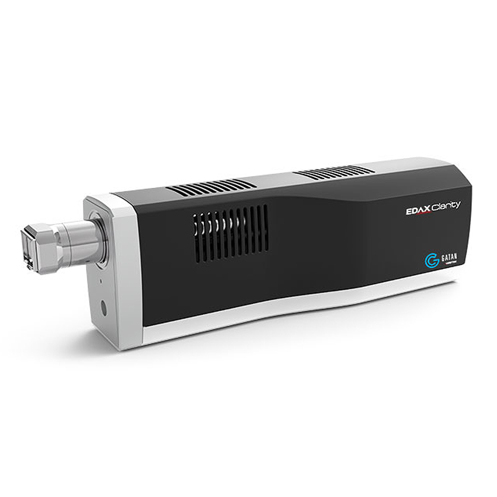
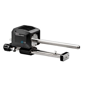
This revolutionary series utilises single-electron detection to provide the high-fidelity EBSD pattern quality and unparalleled sensitivity you expect to advance your research.
- EDAX Clarity™ Plus – Efficient collection down to ~ 7 kV
- EDAX Clarity Super – Optimised for high performance down to 3 kV
EDAX Clarity uses a groundbreaking hybrid-pixel direct detection technology with single-electron detection sensitivity. The incident electrons generate several electron-hole pairs within the silicon upon impact, and a bias voltage moves the charge toward the underlying CMOS detector, where it counts each event. This method is so sensitive that it can detect individual electrons not seen on conventional EBSD detectors that use phosphor screens or light transfer systems.

Coupled with zero read noise, the Clarity provides unprecedented sensitivity and image quality performance. It can successfully detect and analyse patterns comprised of less than 10 e-/pixel. This makes the Clarity ideal for beam-sensitive samples and low beam-dose applications like hybrid organic-inorganic perovskite solar cells and ceramics. Additionally, the Clarity Super is optimised for lower kV acquisition to improve the spatial resolution for fine-grained materials.
Features and benefits of the EDAX Clarity
Beam-sensitive materials analysis
- Reveals never-before-seen structures by using low beam currents and energies to prevent damage
- Eliminates the need for conductive coatings or low-vacuum SEM settings to assess non-conductive materials like ceramics that charge under typical beam currents
- At low beam currents, it obtains high-quality EBSD patterns and maps for investigating the effects of grain boundaries, grain size, and crystal orientation

- Uses high-dynamic-range imaging to ensure excellent EBSD pattern quality
- Enables the collection of extremely sharp EBSD patterns without using phosphor or optical lenses
- Improves spatial resolution at lower acceleration voltages
Reviews
There are no reviews yet.